
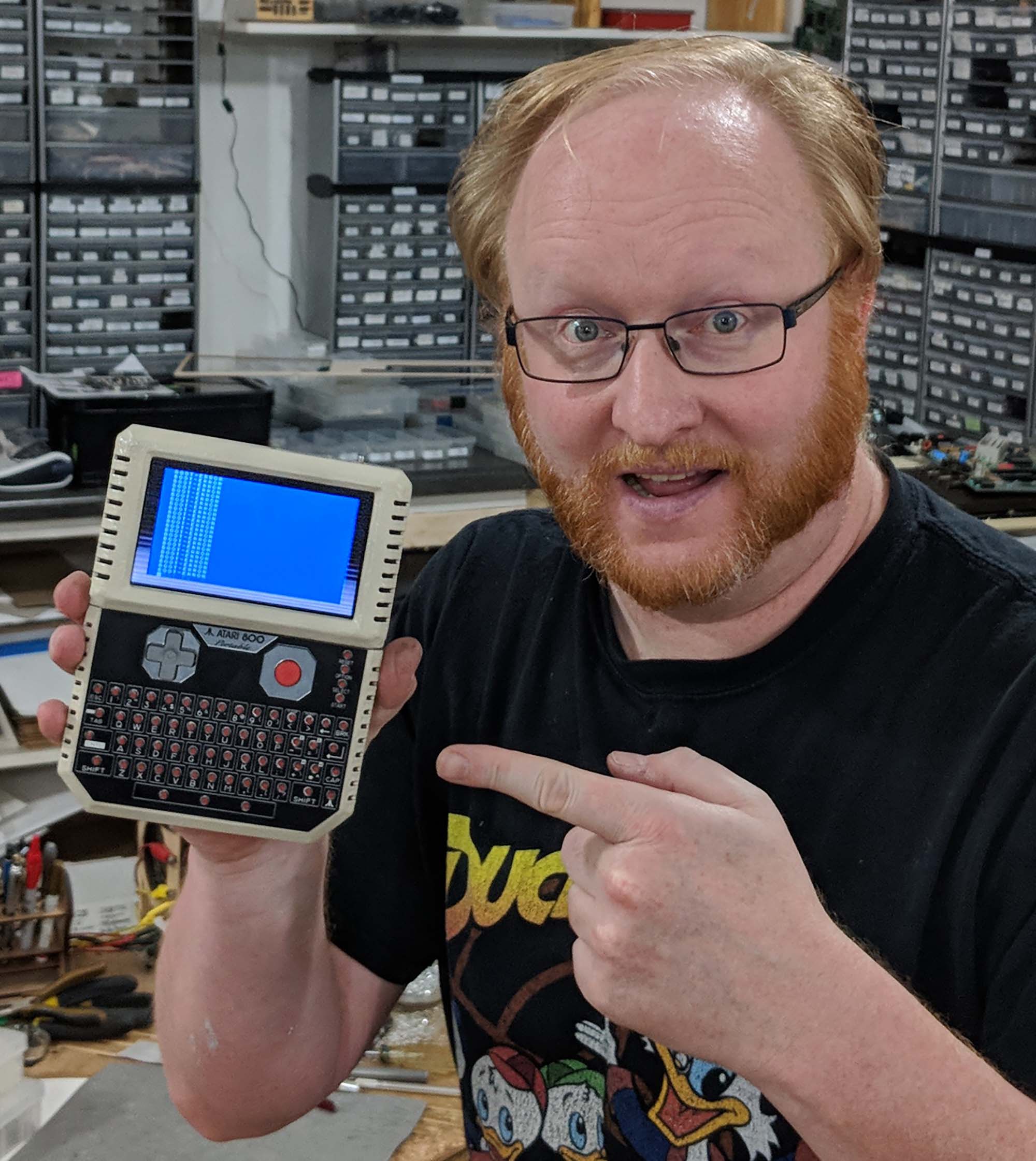
ATARI 800 HANDHELD
Click on any image in this article for a larger version.
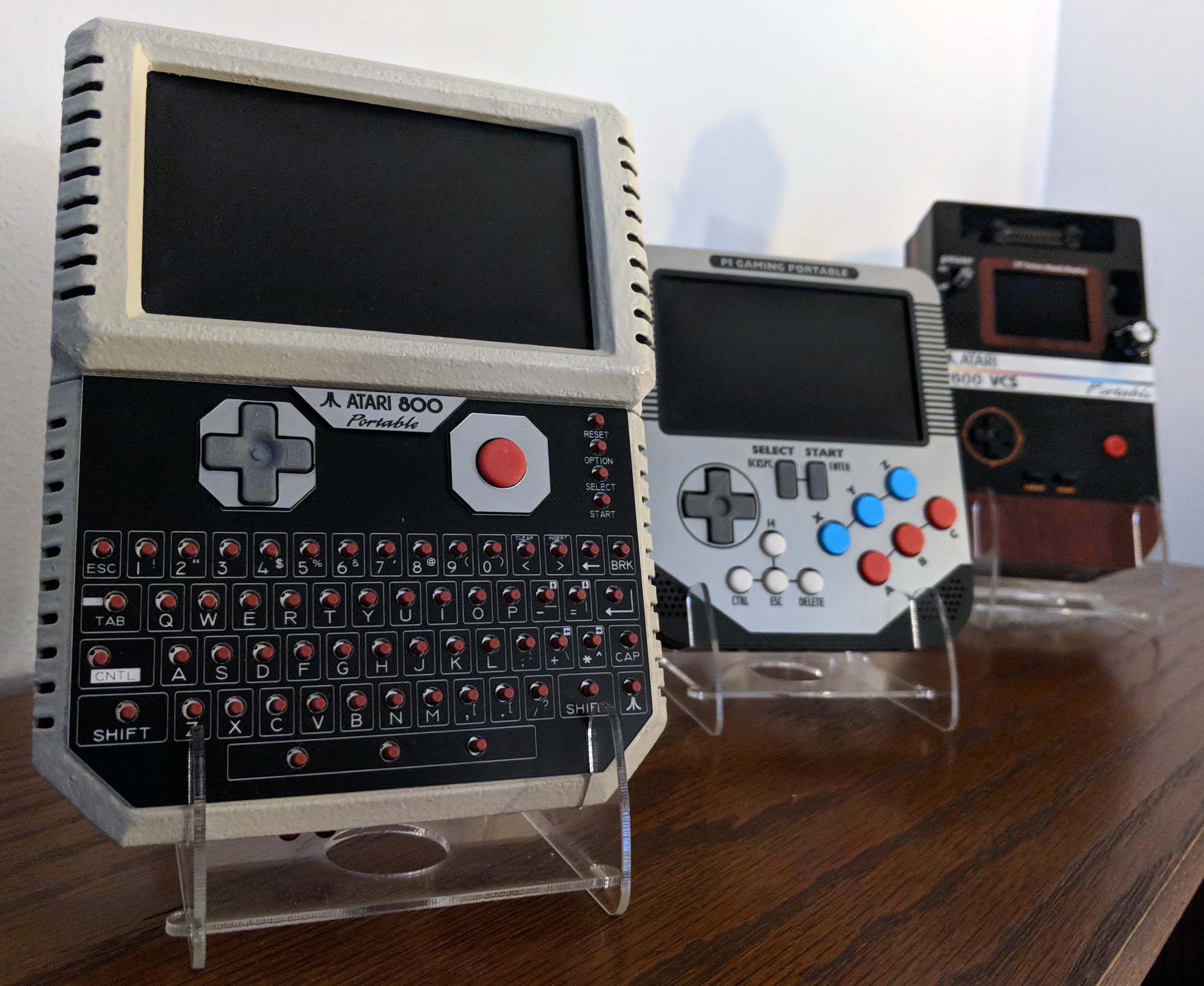
For the final episode of The Ben Heck Show I wanted to do something special. I figured it would be a good time to revisit my favorite old computer the Atari 800.
I’ve done (3) Atari 800 laptops in the past (check the best one here) all based on the Atari 800 XEGS. However they all involved that original motherboard being hacked down a bit and paired with a large screen. Only 1 was battery powered (in a primitive way) the other 2 required wall power.
Since then I’ve done several 8-bit computer projects on The Ben Heck Show. Most of these have involved removing the IC’s from their native computers and either hand wiring a solution or creating a new custom PCB. As the Atari 800 is a fair bit more complex than some of these I’ve done (such as the ZX Spectrum) I decided to spin my own PCB’s to contain as much of the signals as possible with minimum vias and then hand solder whatever isn’t feasible to fit into a home-spun PCB design.
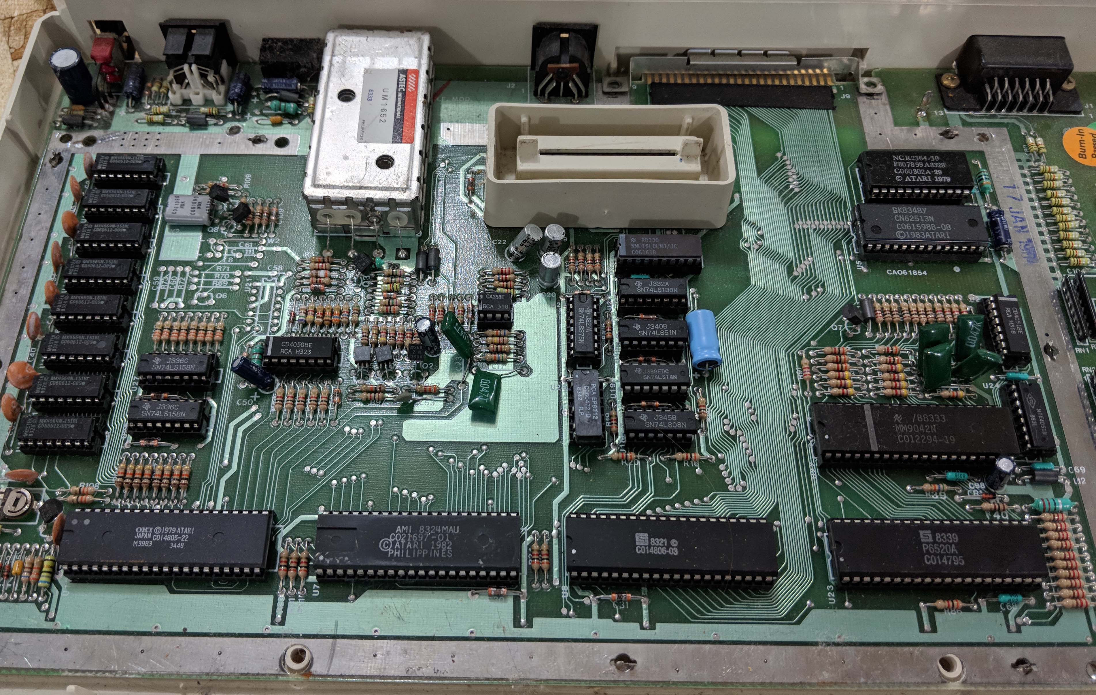
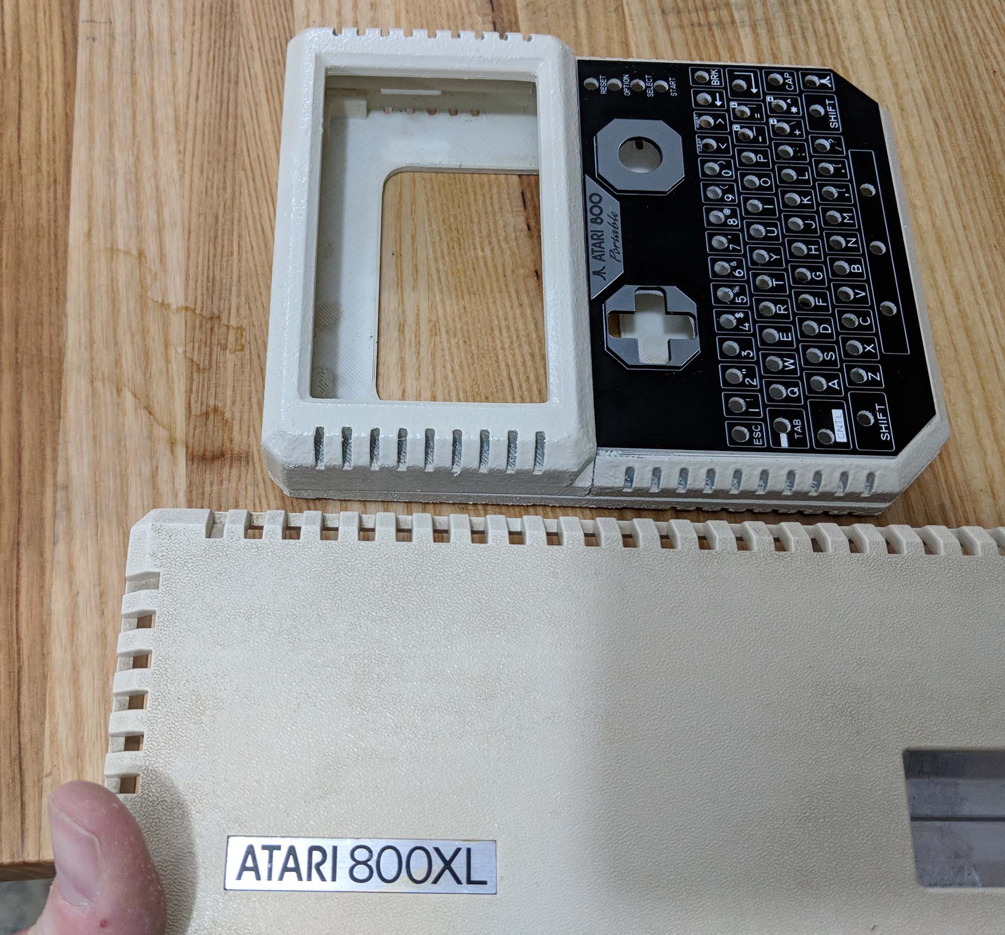
I started with both an Atari 800 XEGS (which are getting more expensive on eBay!) and an Atari 800 XL (which are cheap and plentiful). Since I was rebuilding a board from scratch I wanted extra copies of the IC’s so I could test faults as I went – always good to have a working reference. This came in handy during assembly as I could probe the working 800XL and the new system with my scope and see if the signals matched.
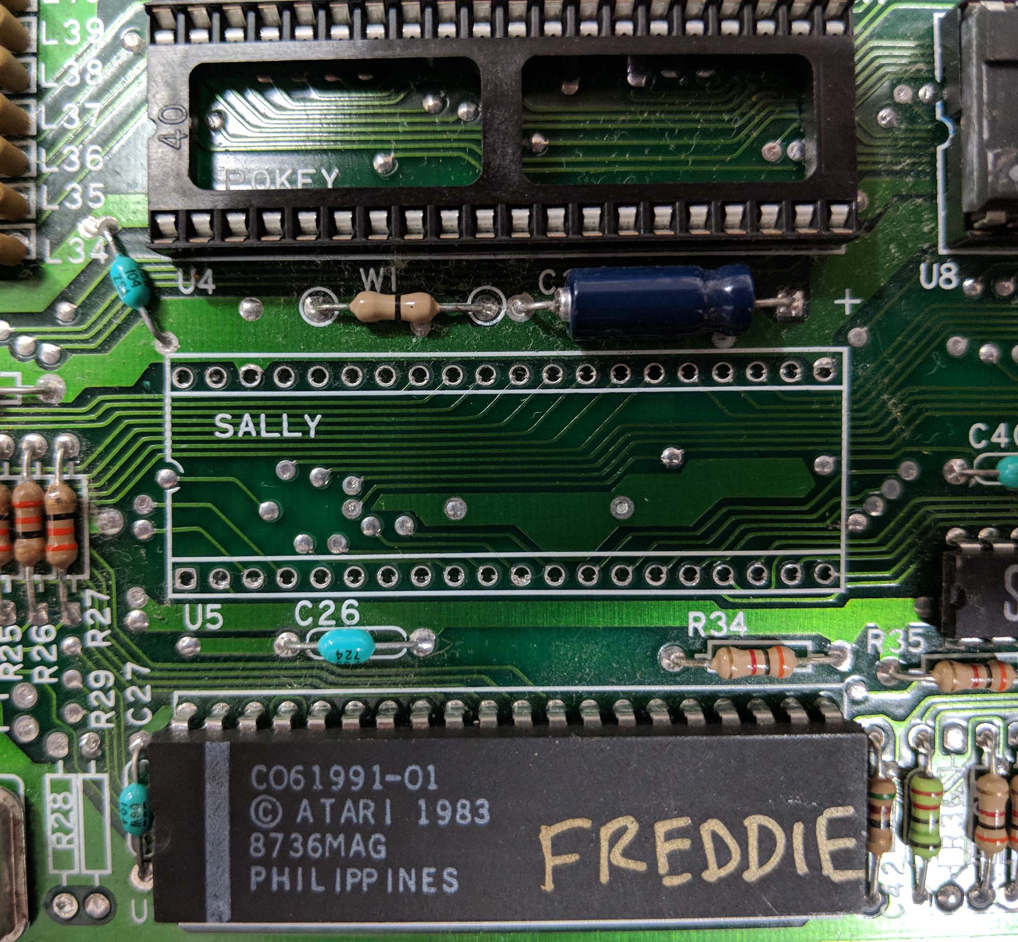
The XEGS chips were soldered directly to the PCB because sockets cost money! This was a cost savings measure that happened during the 80’s. I desoldered each IC and installed sockets so I could test out the chips. I wanted to make sure they were cross-compatible between the 800XL and the XEGS. That way I had backups, and also knew that probed signals on the new board would match those on the still-working 800XL.
PCB DESIGN & MANUFACTURE
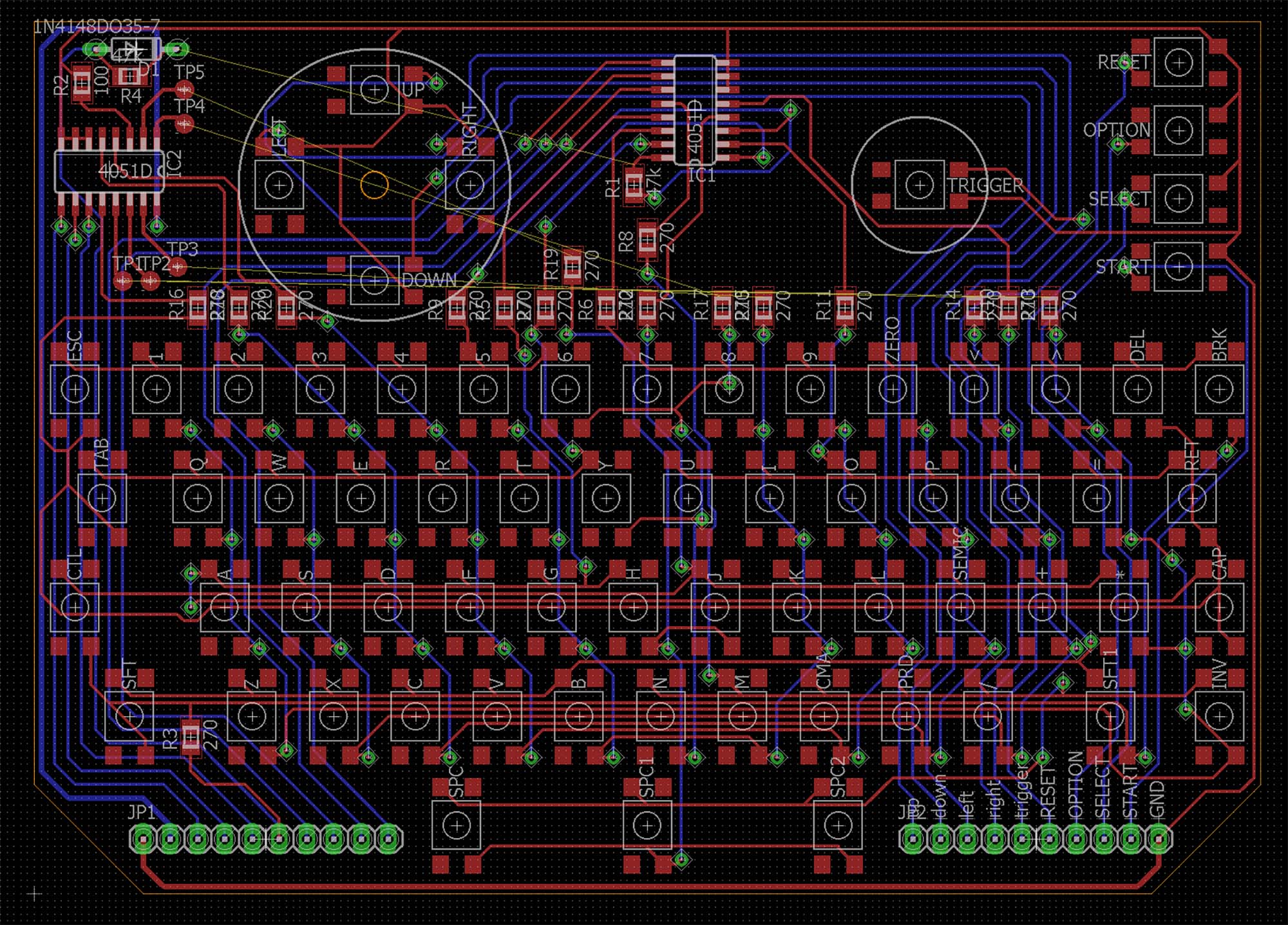
Atari 800 schematics aren’t the easiest thing to thing to find online, at least in their complete form. Luckily I came across a site that had them all, including one for the Atari 800 XEGS. Using this I was able to draw my own schematic in Autodesk Eagle.
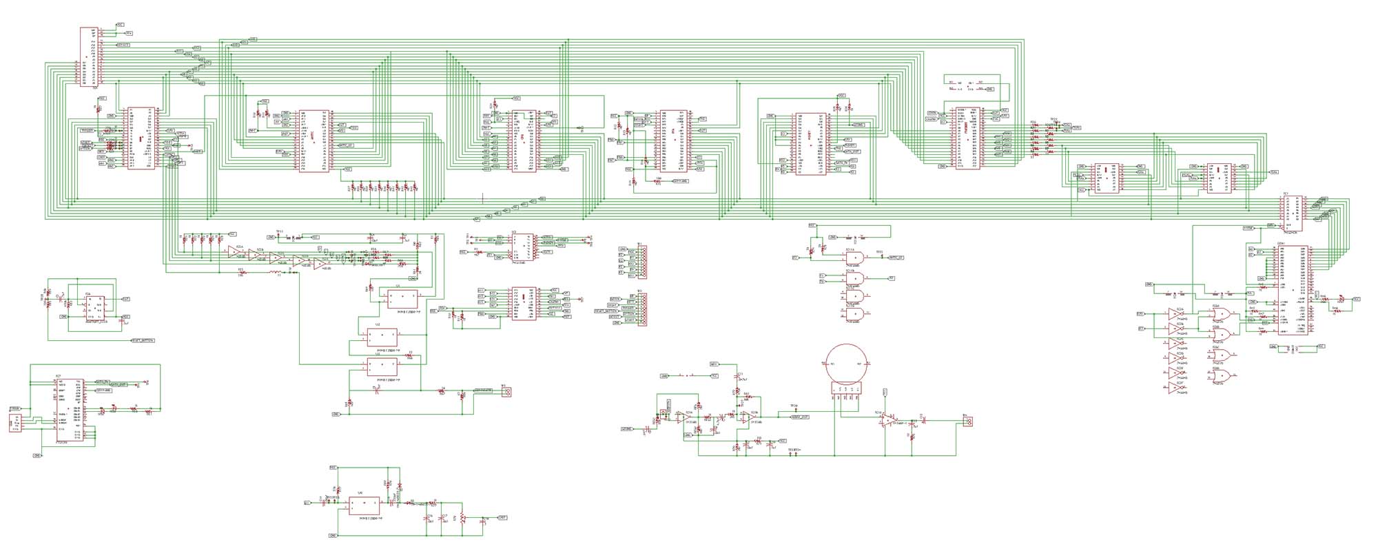
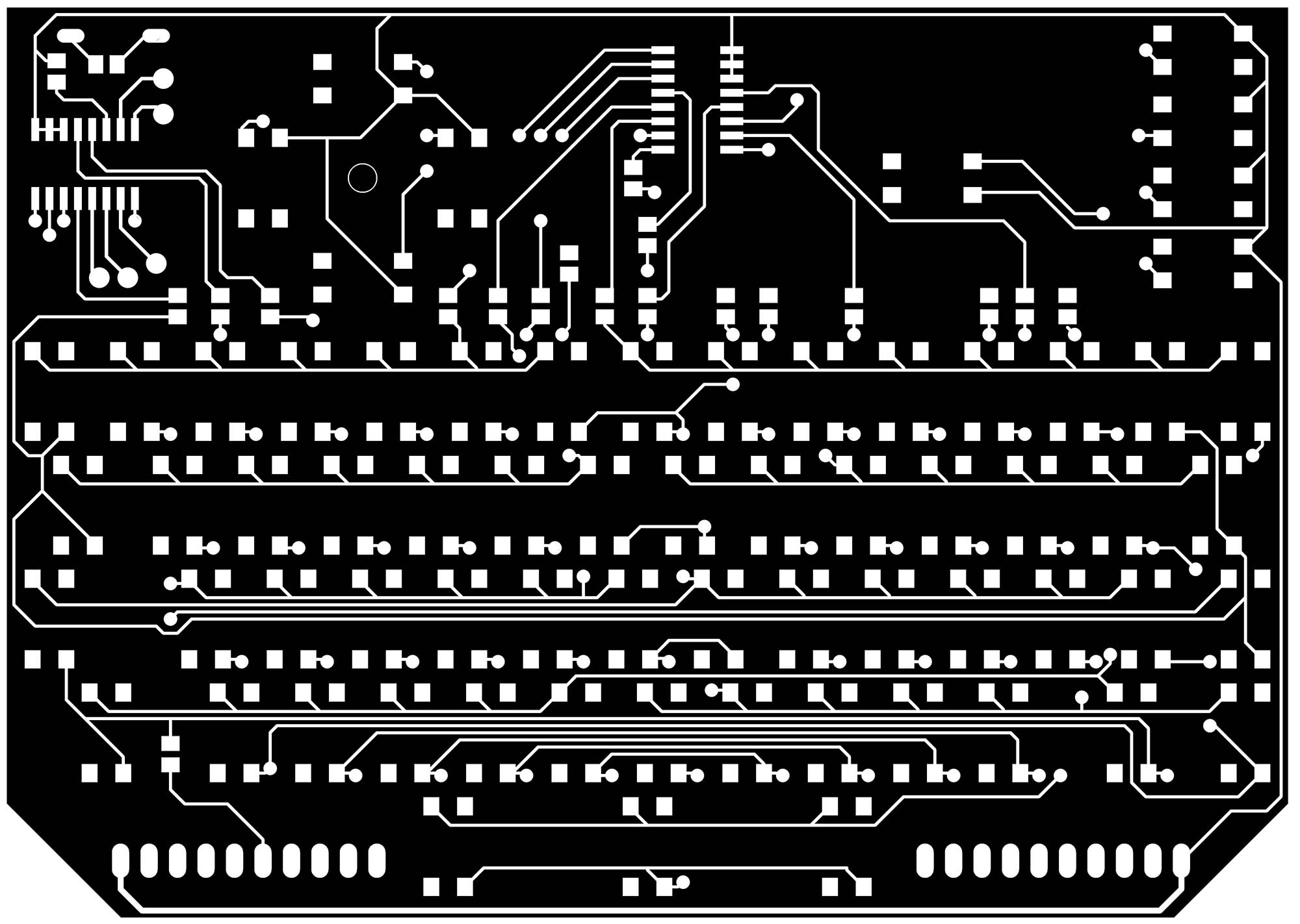
Laying out the electrical schematic was the easy part. Once that was done, I had to rout all the traces!
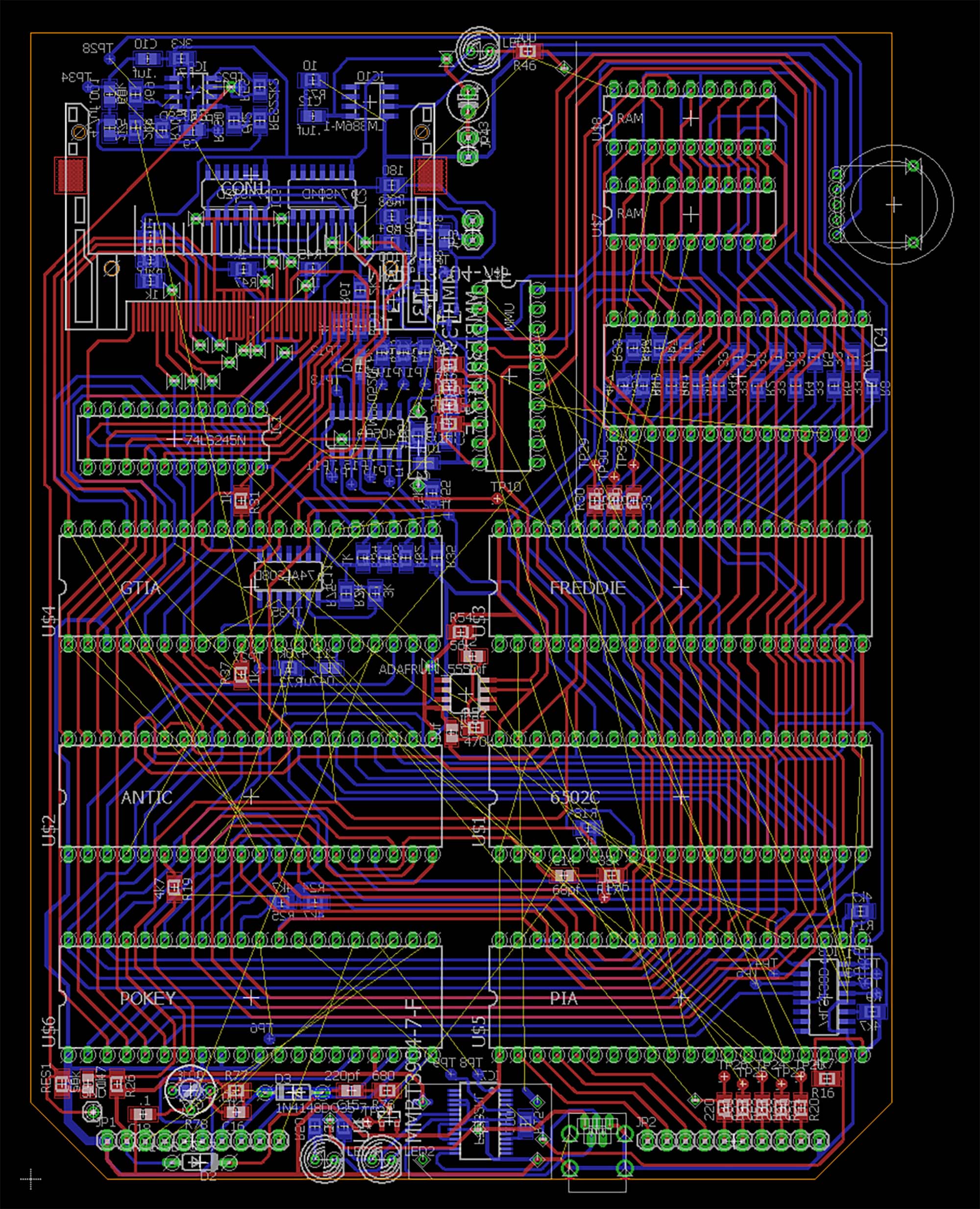
This is the board as viewed in Eagle. Since we were making this board ourselves using Laser Paint ™ I knew it wouldn’t have the accuracies of a board house. I also had to limit my use of vias because they’d have to be threaded by hand and wouldn’t be flat, which could be a spacing problem if a component was installed over them.
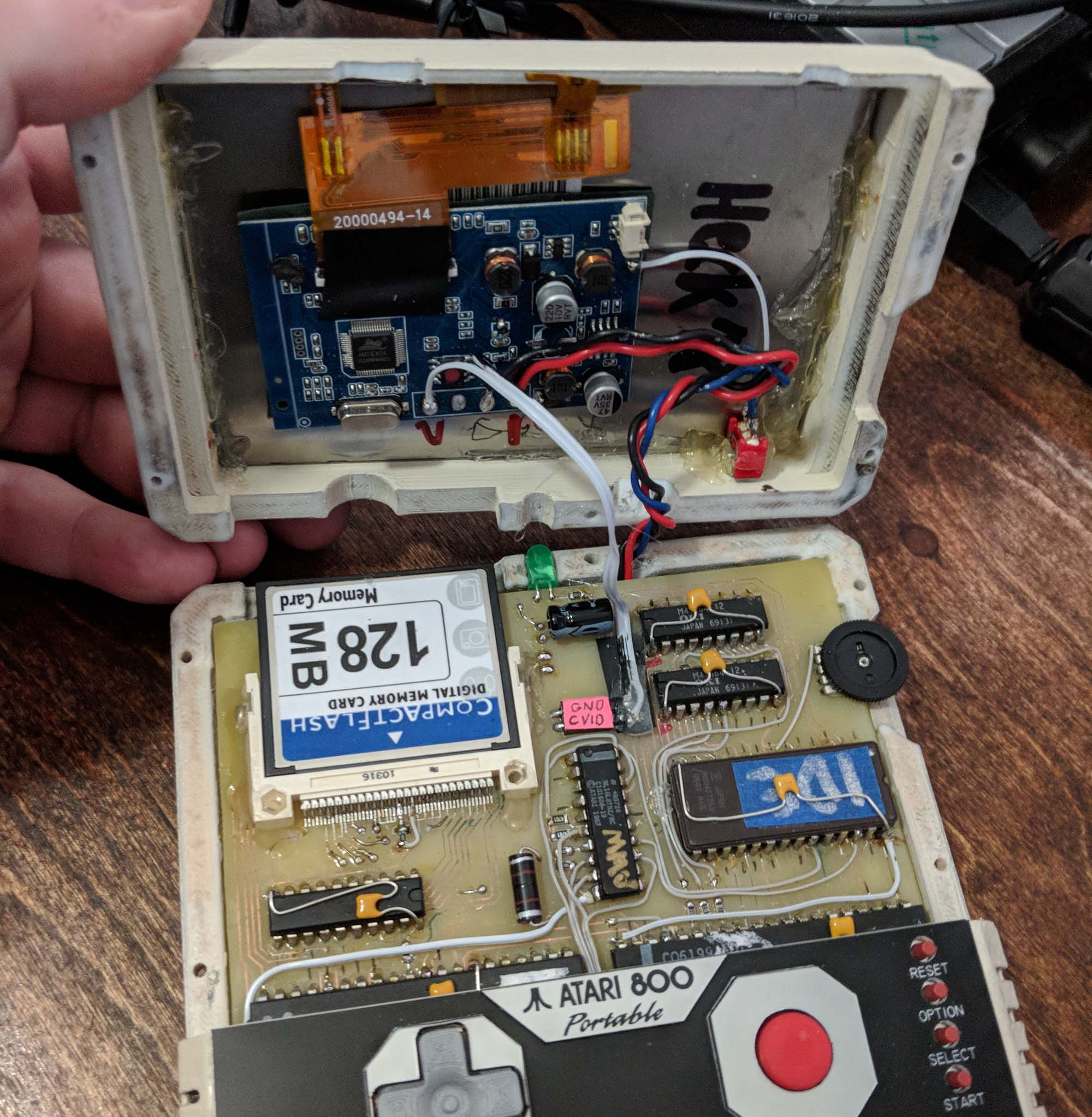
I was able to rout about 95% of the board within the tolerances we had. I used IC pins as vias (to transfer a signal from one side of the board to the other) as much as possible. Note how almost all of the normal vias I did have to use are around the CompactFlash card. The address and data buses loop around the board forming a “U” shape. It worked out pretty well!
The yellow lines are “air wires” – signals that haven’t been traced. At a certain point it became faster just to wired them manually than to try and squeeze any more tricks out of the space we had left. Running traces between through-hole pins is a great way to save space and was well within our tested tolerance levels for custom in-house double-sided PCB’s.
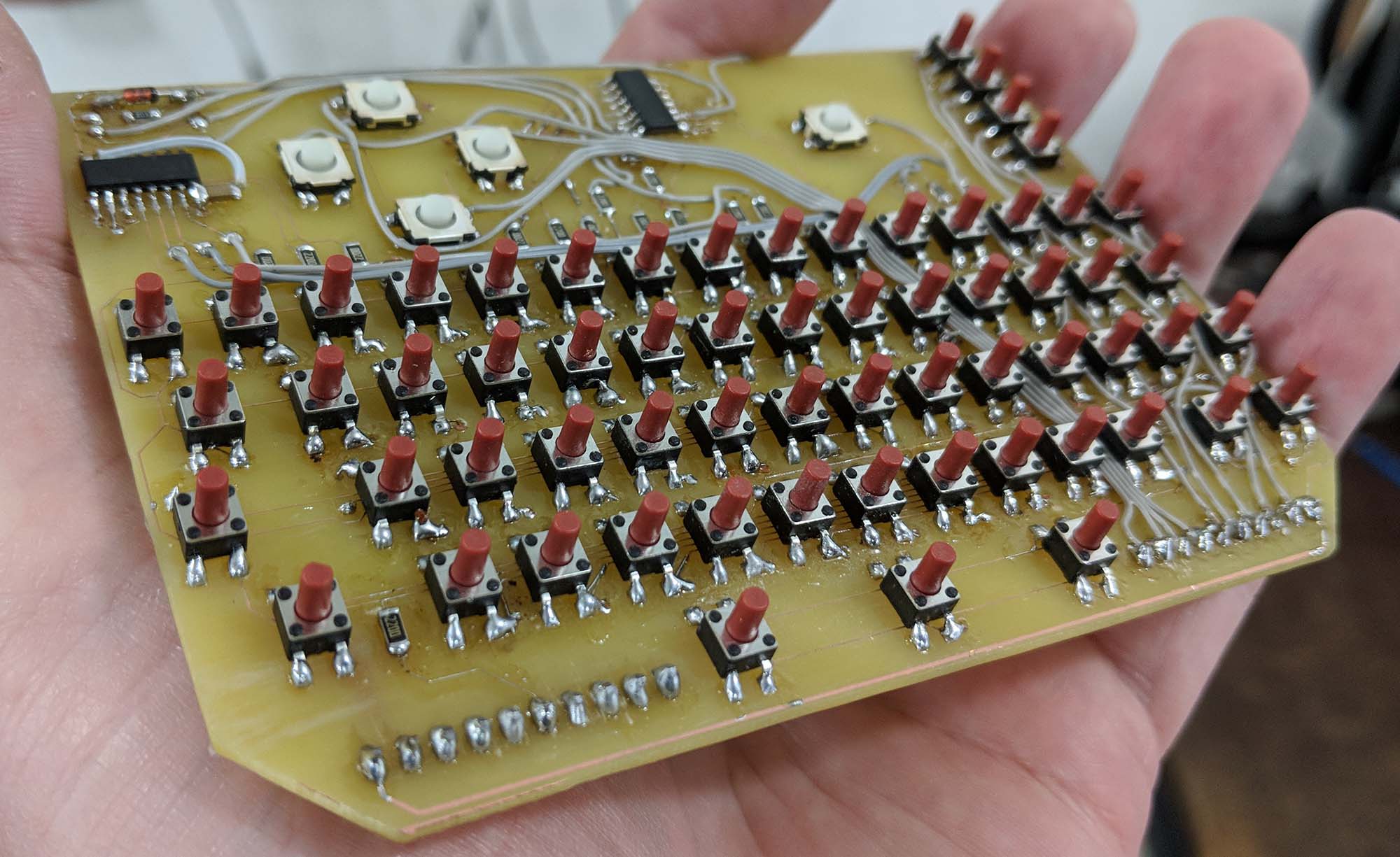
We also made a custom PCB for the keyboard that plugs into the main motherboard. This is very much like the detachable keyboard on the Atari XEGS! It also includes Joystick 0 and Reset, Option, Select and Start keys which are not part of the keyboard matrix and require their own wires.
We made the keyboard PCB first since it was smaller, self-contained and simpler than the main motherboard. We wanted to see if the new board-flipping method for Laser Paint gave us the tolerances we wanted… it did! By using pegs to secure and flip the PCB inside of the laser cutter, we were within about 10mils accuracy when flipping to side 2. These are both double-sided homemade PCB’s.
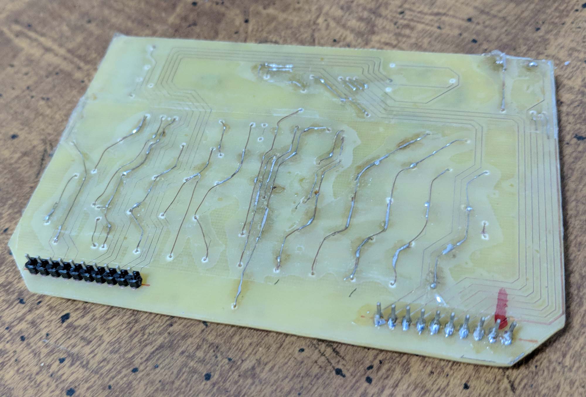
We achieved the accuracy we needed but some of the rear copper traces were destroyed in the bath. I fixed this with a lot of thin solid core wire and put packing tape over it to avoid shorts. We’ll take more care when etching the main board!
I then attached the keyboard PCB to the XEGS to see if it worked. I did come across some weirdness in the way the columns/rows were addresses, but was able to fix it with a few wire bodges. Not sure if it was me or the schematic, but now it works.
Now that I knew the double-sided PCB could be made to a good tolerance I finished designing the motherboard and we laser-painted that as well.
Perhaps I should describe Laser Paint ™. It is a method of making your own PCB’s that Felix and I came up with:
- Paint your copper clad board with 2 coats of Krylon
Spray Paint (any color will do 🙂
- Let it dry overnight. In a pinch a couple hours is enough, but the paint may fail.
- Prepare a “black and white negative” of your PCB. White where you want copper to be, black where it shouldn’t. I make mine by exporting PNG’s from Eagle and adjusting colors in Photoshop.
- Stick painted copper clad in your laser cutter. Using standard raster-engraving settings, burn away the paint at the highest DPI possible. Use the air assist if you have it to push particles away from lens. For best results do 2 passes.
- Clean away the atomized paint using 90% rubbing alcohol. Be sure to scrub lengthwise along traces. Once the copper looks clean and shiny you’re ready. The alcohol will affect the paint if you scrub it long enough, but really you’re just getting rid of the paint residue here (this is why 2 passes is a good idea – much easier to clean)
- Etch the board using the solution of your choice. The etchant has no effect on the paint (unlike the rubbing alcohol) so it’s OK to agitate the etchant bath or even scrub with to speed up the process.
- Once the copper has been removed, clean the board and remove the paint using acetone. Viola – you have a laser-made PCB!
- Cut the PCB to shape using a band-saw.
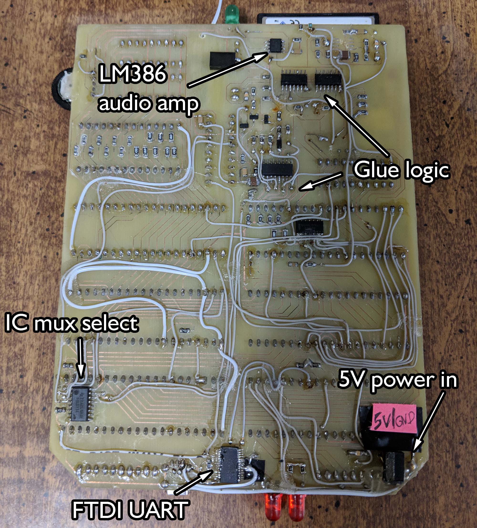
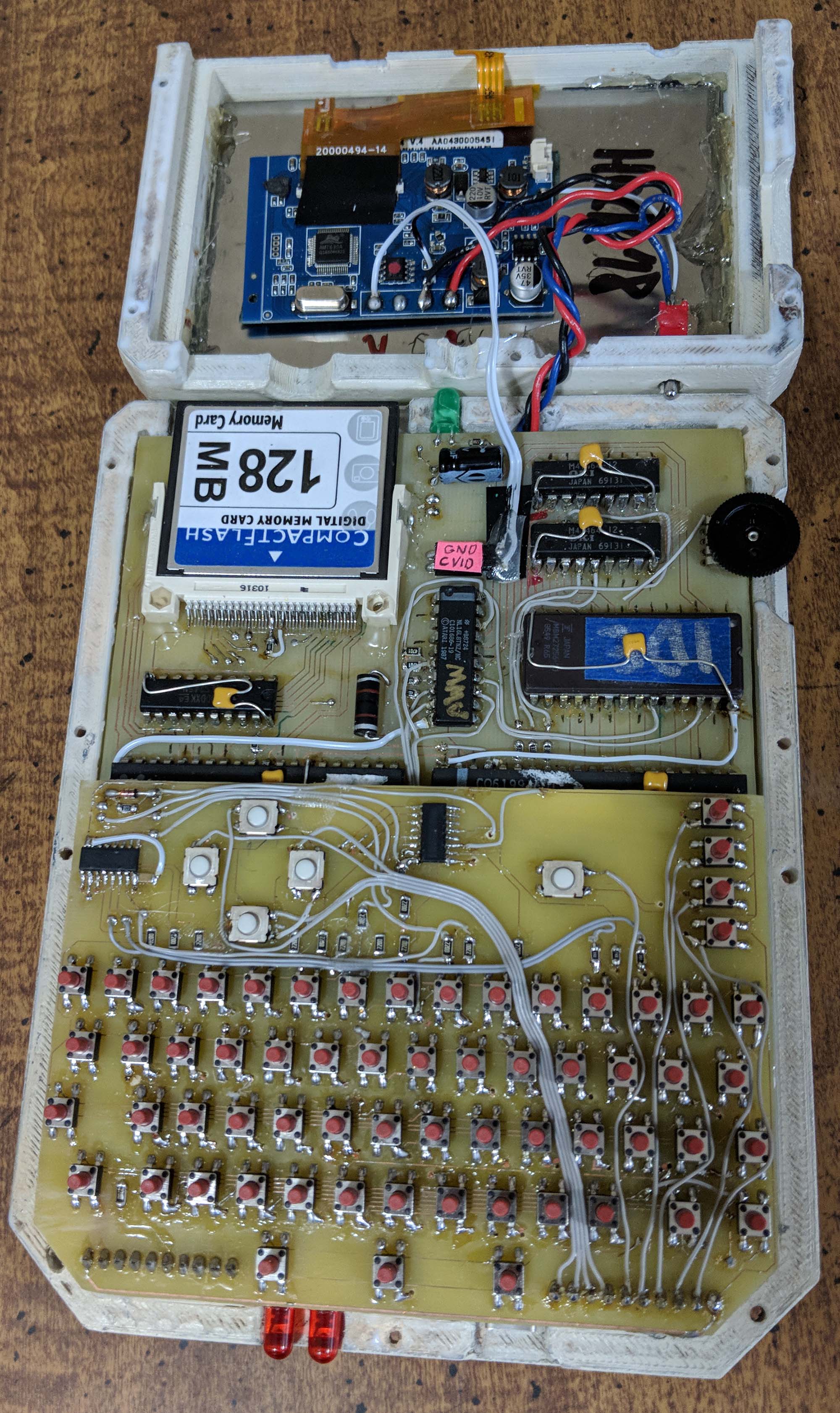
STUFFING PCB
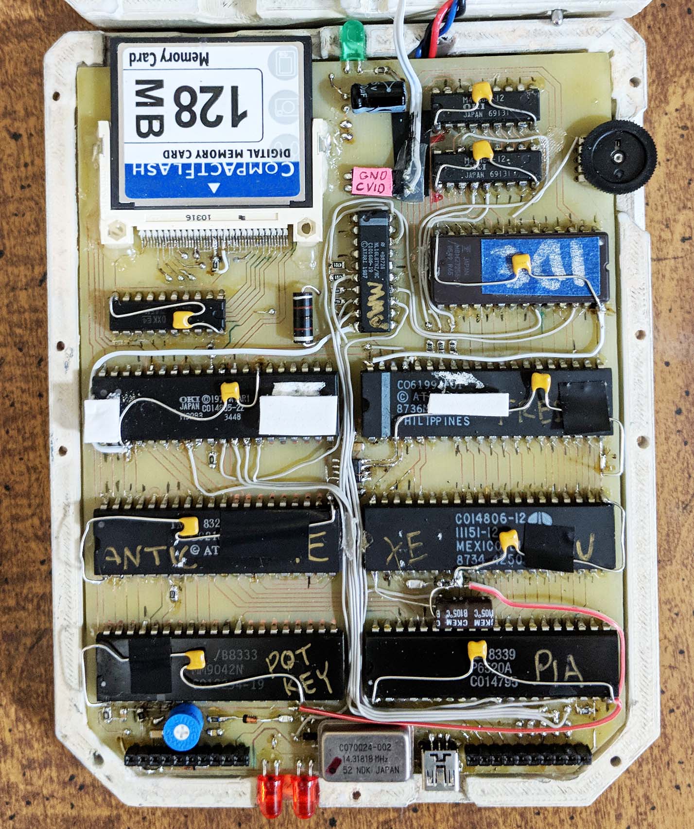
It was time to start stuffing the PCB! To help out in troubleshooting, I bent out the ground leads on all of the top surface capacitors (the yellow things) to give myself lots of clamp points for the oscilloscope. The white squares are a foam backing for the keyboard. The LCD is a cheap 4.3″ backup camera from Amazon.
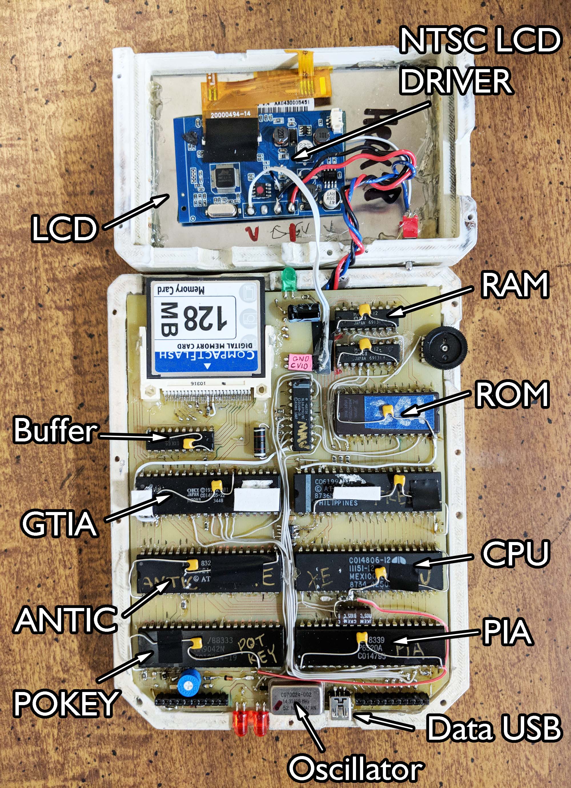
There were about 80 total manual bodge wires which sounds like a lot but wasn’t too bad. Again I was working within the limits of our homemade PCB’s so I couldn’t use a lot of vias or other tricks one can with a “real” PCB.
Most of the errors I found when probing it with the scope were the result of airwires I forget to wire, so I went back to Eagle and did a Design Rules Check and copied the airwire error messages into an Excel spreadsheet and went through them one-by-one.
Other issues included the op-amp not being required for the audio circuit, changing the resister values on the video luminance circuit and fixing a connection I didn’t realize I needed on the FTDI chip.
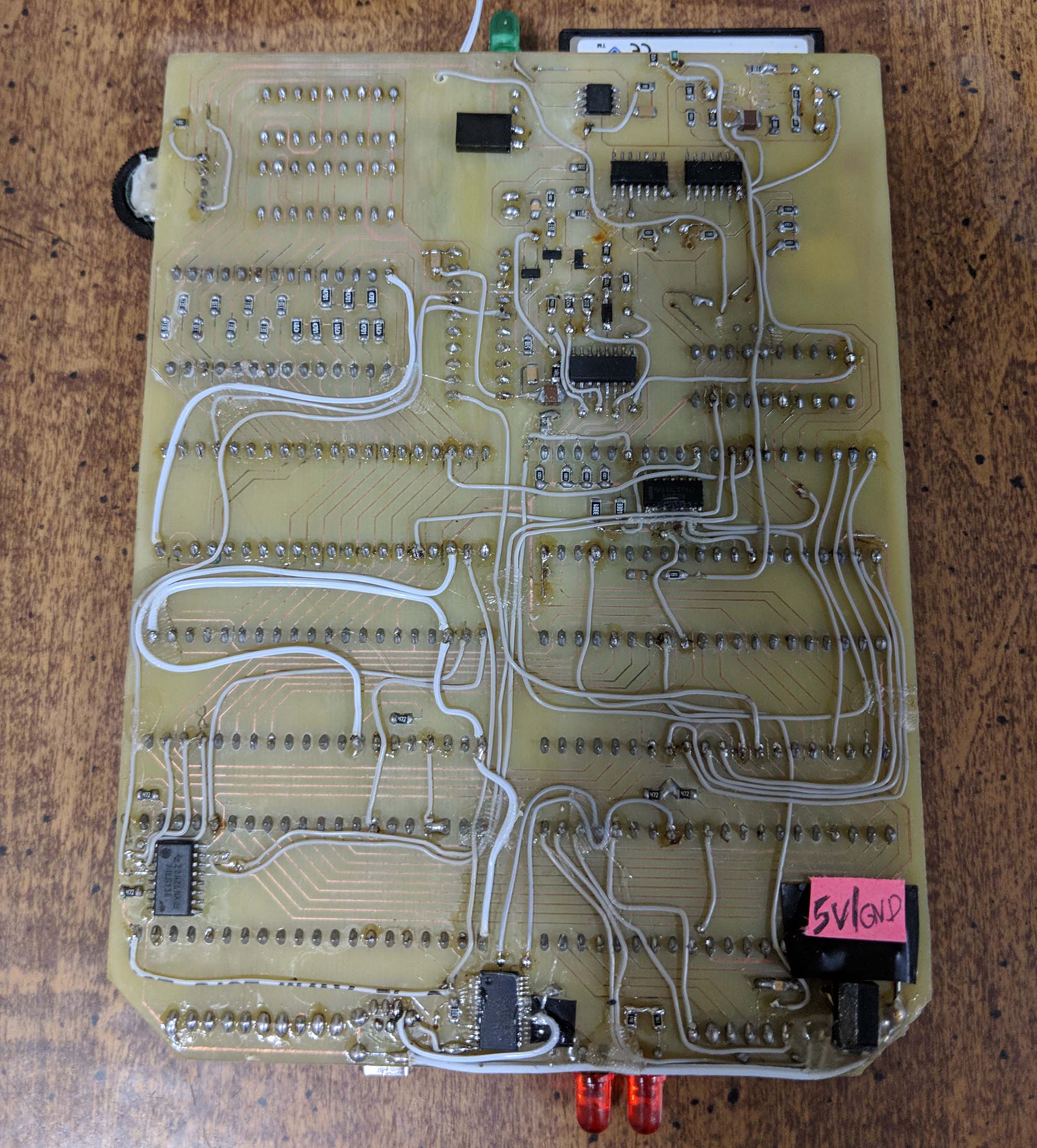
Most of the glue logic we needed for memory mapping and other functions has modern surface mount equivalents so all of those parts are mounted on the bottom to save space. The only modern part I used a through-hole version of was the data buffer for the CompactFlash card because I didn’t have a surface mount version on hand.
CASE DESIGN
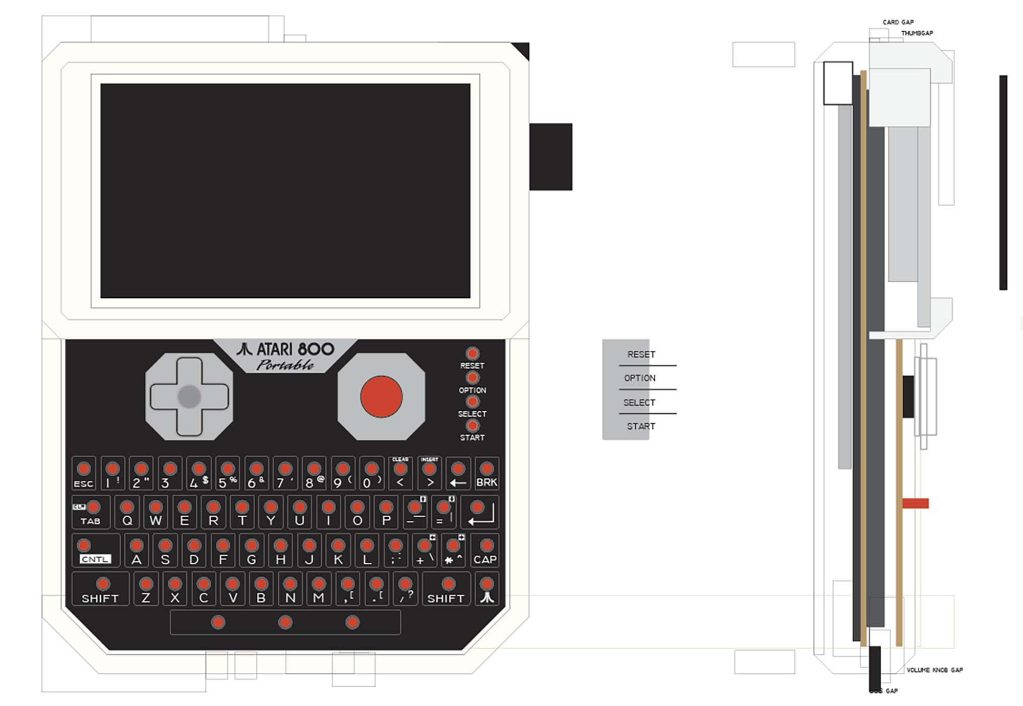
To design the case I exported the PCB from Eagle as a DXF. This imports easily into Adobe Illustrator. I then used Illustrator to figure out the basic look of the unit and the major components. I drew this from 2 angles – front and side. By figuring out most of the depth information here I’ll save time when I move onto 3D.
Basic concept is to take the outline of PCB + .031″ for a gap and then + .25″ for the side walls. A quarter-inch side wall will have plenty of room to fit countersunk size 2 screws (all units Imperial).
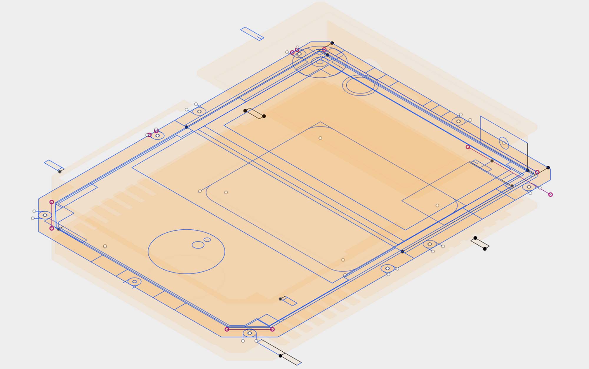
I exported the DXF’s from AI and brought them into Autodesk Fusion 360. 3D design involves a lot of 2D sketches being extruded into 3D shapes. I extruded all the depth information that I gleaned from AI into solid bodies in Fusion 360. These will form the basics of our 3D prints.
Here’s the 3D component view in Fusion. Notice how the keyboard and label plate is missing – this will be done in 2D with AI and the laser cutter so there’s no need to design it here in 3D. At this stage I added a lot of extra detail like edge chamfers and air vents to match the look of the Atari 800XL.
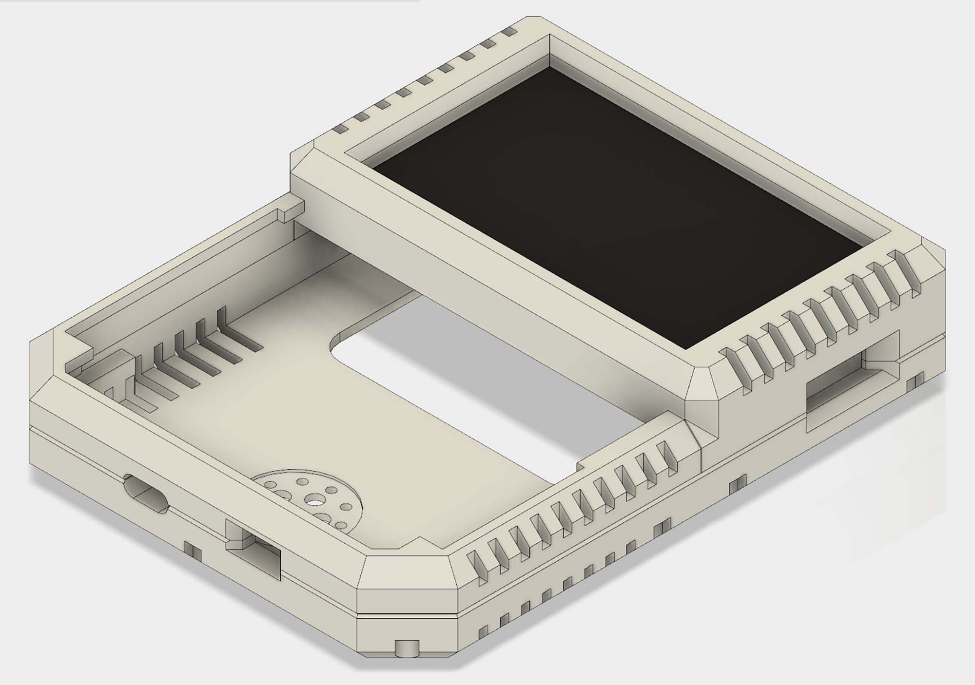
The casing was printed with my Makergear M2 3D printer using white PLA. Since we were planning on painting it anyway (and were crunched for time as usual) I used low resolution layer height. The D-pad and trigger buttons were printed on ABS using my old trusty Makerbot
. I often use multiple printers for a single project but I try to do things in groups – ie do all the case parts with one printer, and the buttons and inserts with another.
FINAL ASSEMBLY
Felix found a color of Krylon spray paint at the hardware store that matched the Atari 800XL. That computer was never truly white… more of an off-white.
We used more coats of paint than usual to cover up the 3D layer striations, and used a sponge to give the final layer a classic 80’s texture.
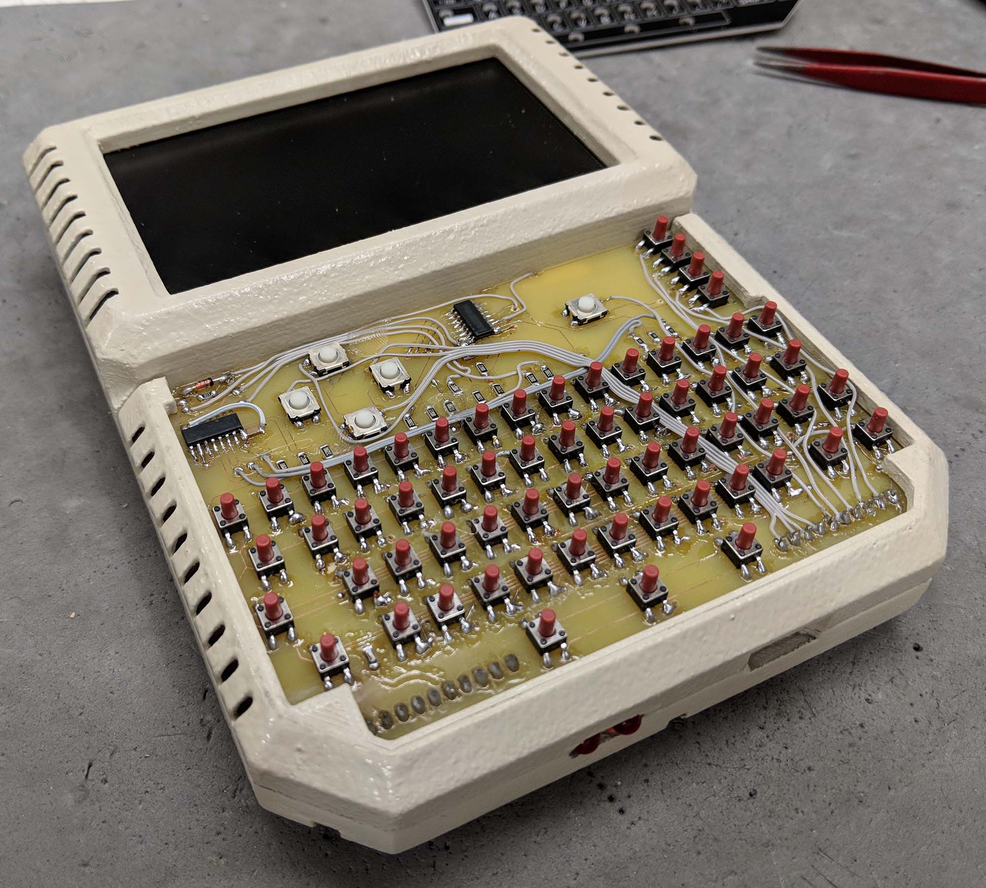
Did some test fits of the interlocking PCB’s. Notice the extra gray bodge wires going from the D-pad to the header area. Some of the traces were lost during the etching of this PCB, but it was faster to hand wire them than to re-do the board.
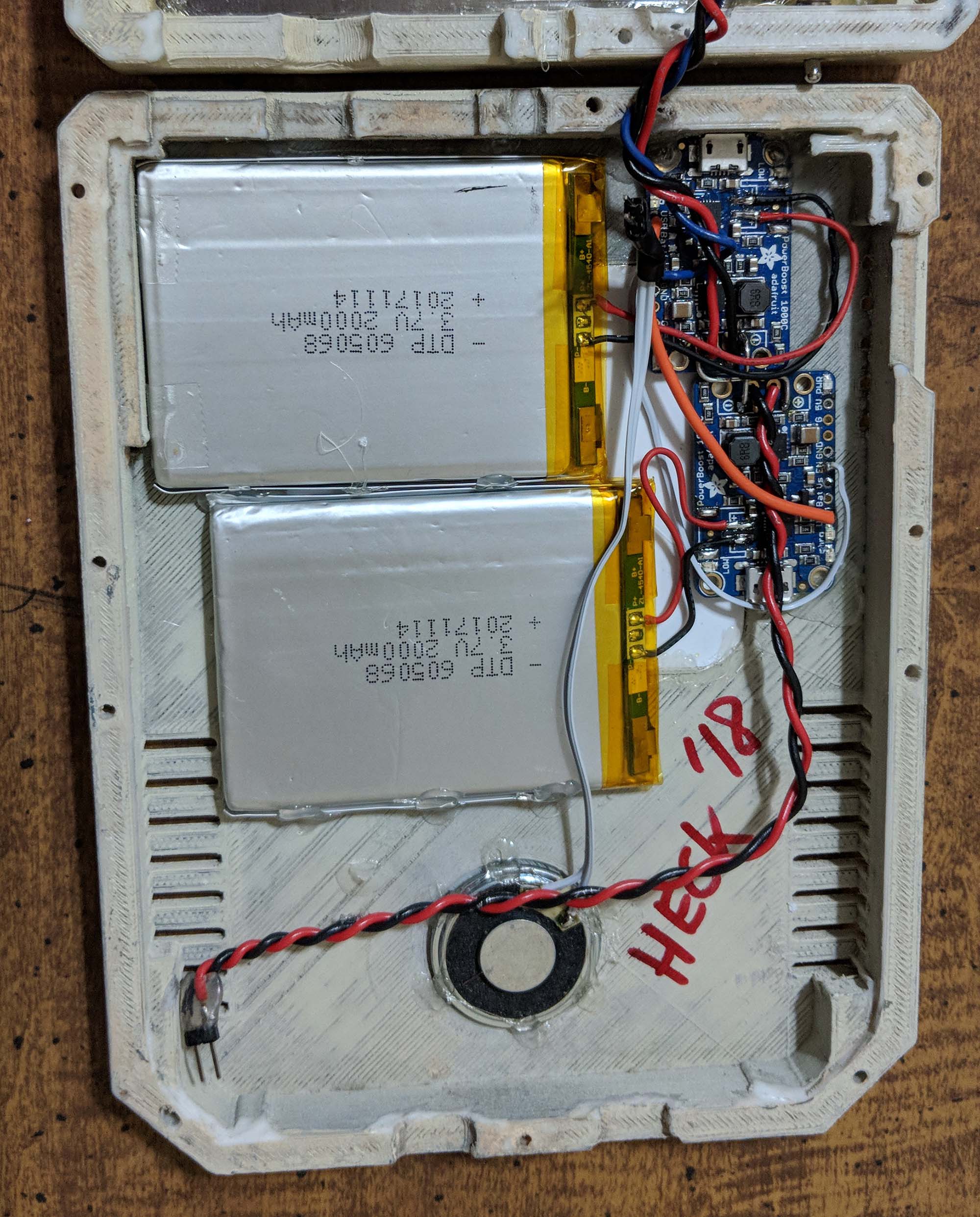
The Adafruit 1000C Charger/Boost is a great package we’ve used many times, but this project was a little too much for it. Turns out the boost part of the circuit tops off around 800mA so our 950mA device wasn’t fully working. Felix read online that it was OK to use 2 in parallel so that’s what I wired up. Not the best solution but a fast one. I estimate about 3 hours of battery life in this config (remember the current draw on the 5V line is less than the actual battery discharge at 3.3V pre-boost)
Changing up our battery plan did require the rear half of the case to be re-printed about 1/8th of an inch thicker to fit the extra batteries.
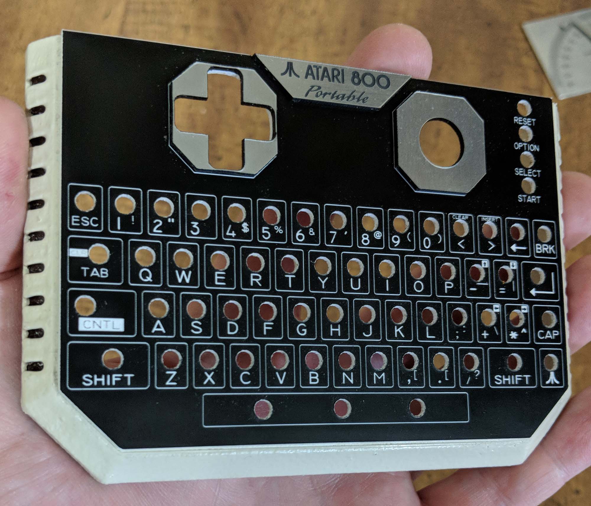
The keyboard plate was laser etched and glued into place to finish up the unit!
CONCLUSION
Gaze upon the glamour shots of the unit below! Click on the images to see the full-sized version. Enjoy!
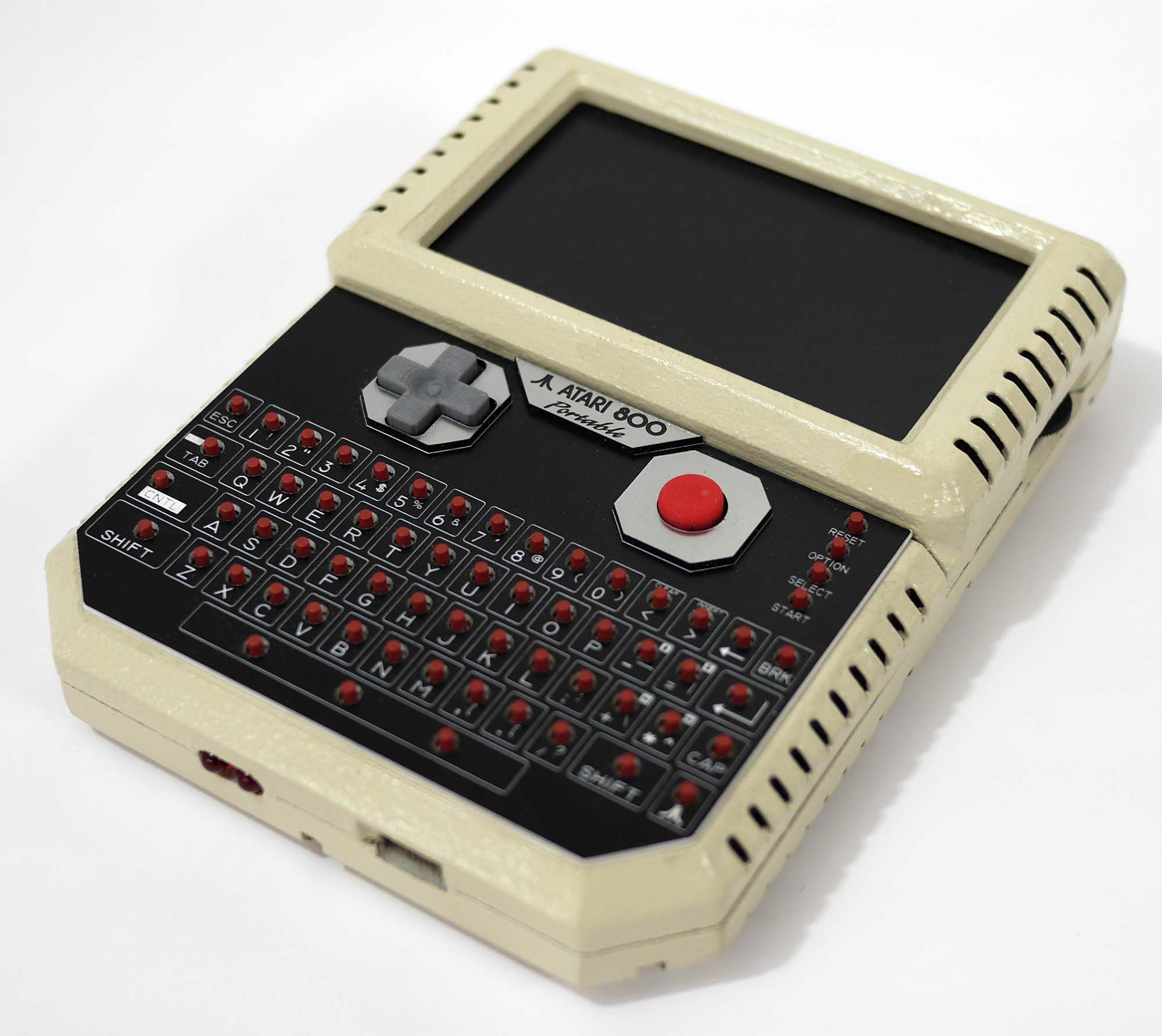
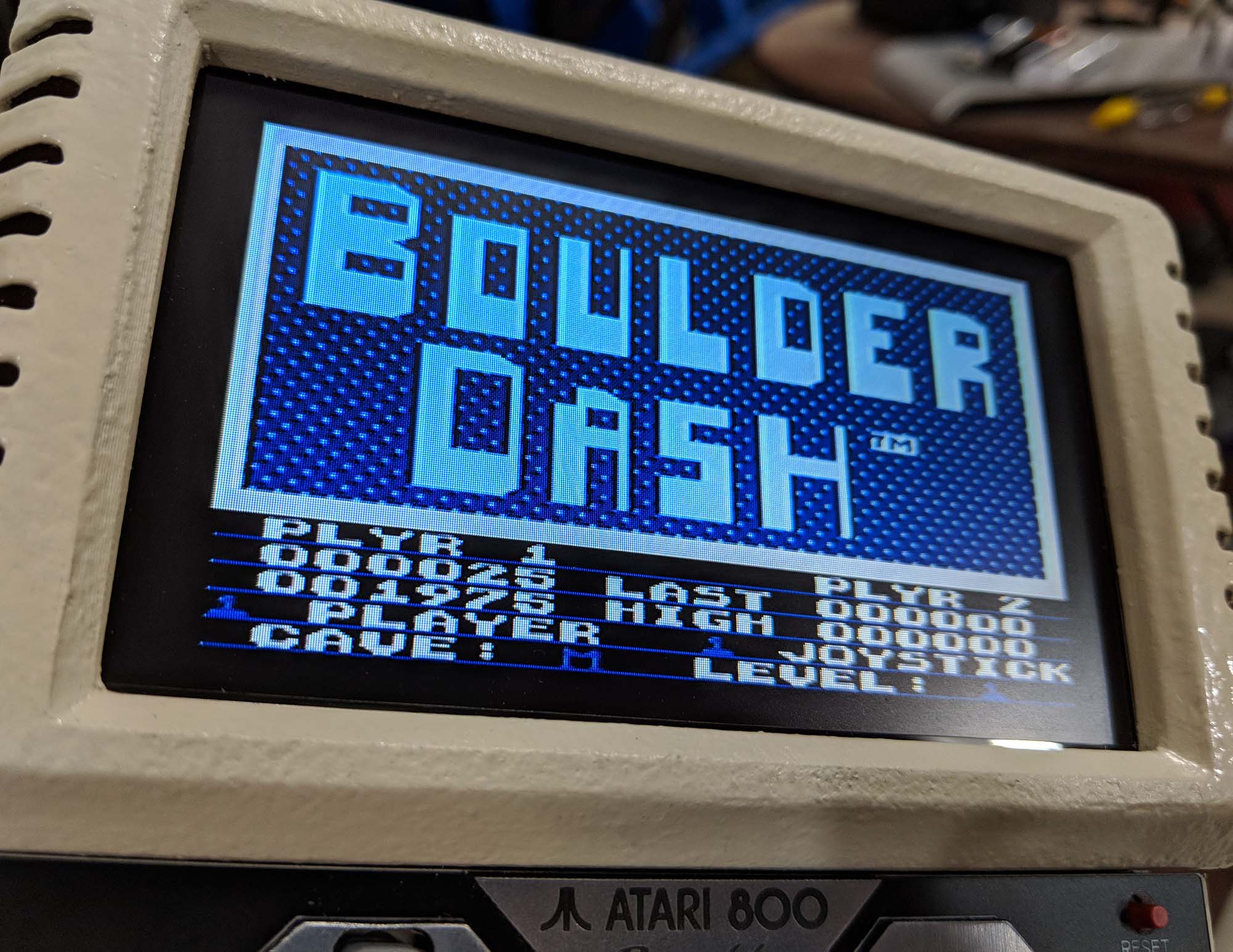
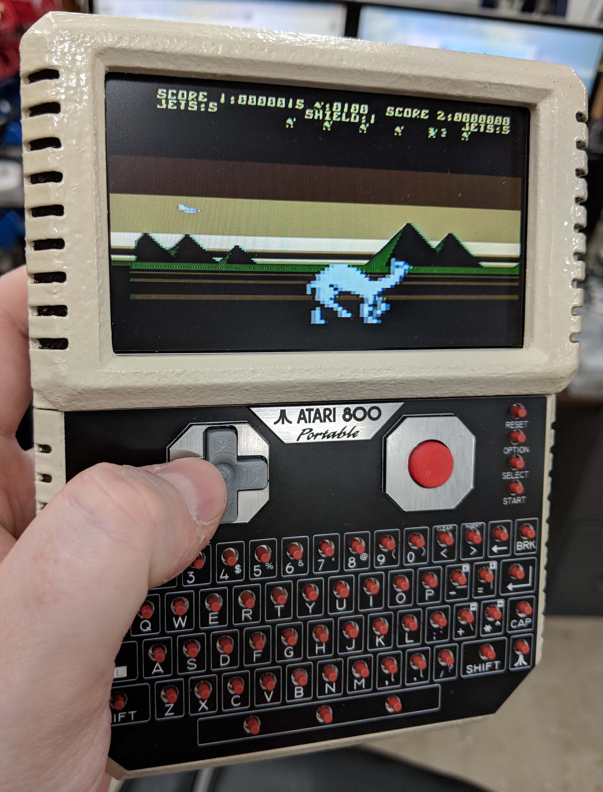
4.3″ LCD screen. It’s NTSC, for better or worse, but looks pretty sharp.
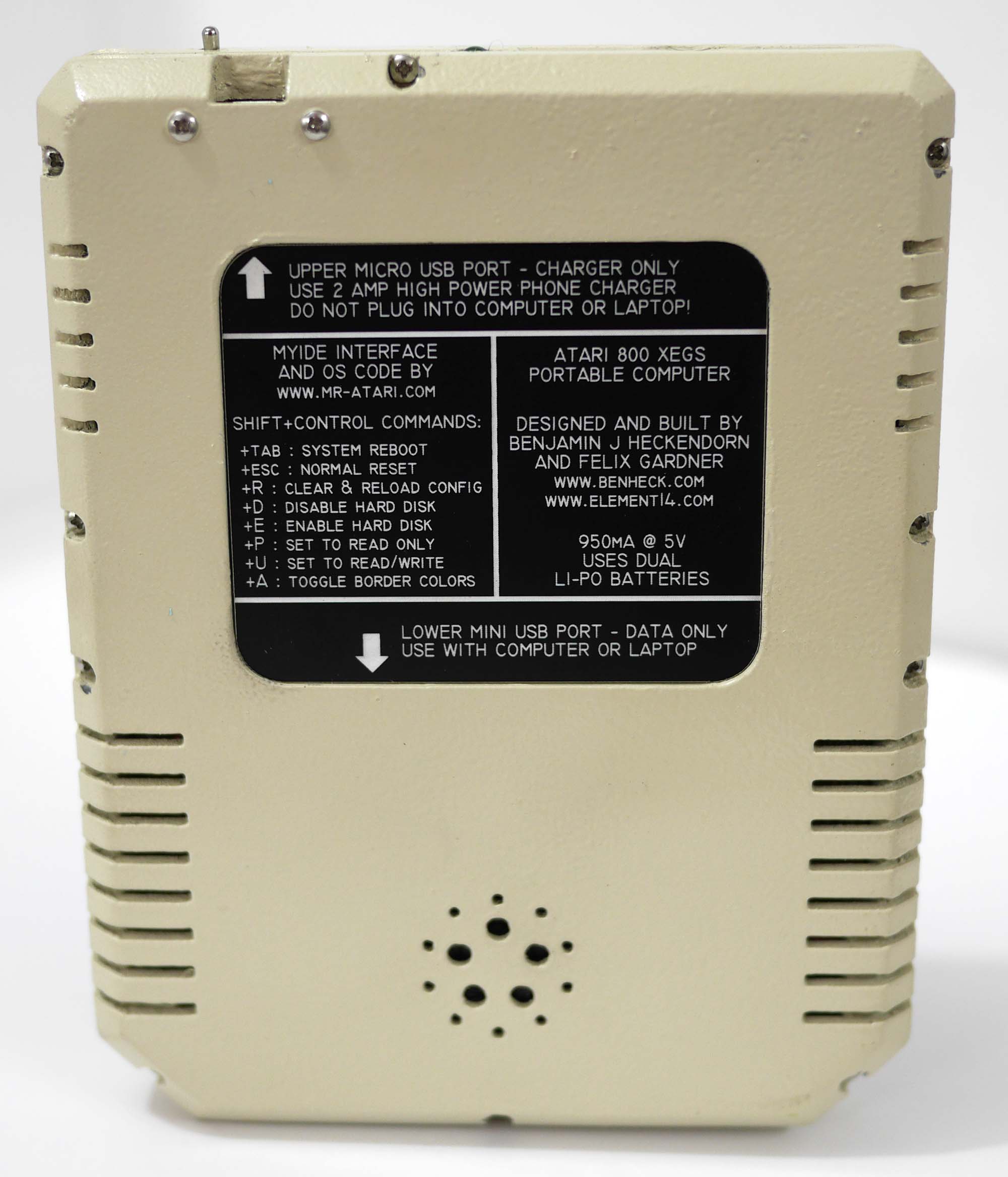
There are (2) USB ports on this thing. The top one is a USB micro and is for charging only. You need to use a cell phone charger as it draws about 1.5 amps! (a computer’s USB port tops off at 500mA)
The lower port is USB Mini and is connected to the FTDI UART chip on the new motherboard. The POKEY chip on the Atari communicates with disk drives and other peripherals at 19,000 baud serial rate. Combined with the FTDI serial-to-USB converter it becomes compatible with modern computers! Using a program like RespeQt you can use your PC as an emulated hard drive and load software to and from the real Atari hardware. I used this to boot up the system and write DOS files to the CompactFlash card.
Hooking up an Atari to a modern PC is quite easy using any FTDI breakout board, check here for more information!
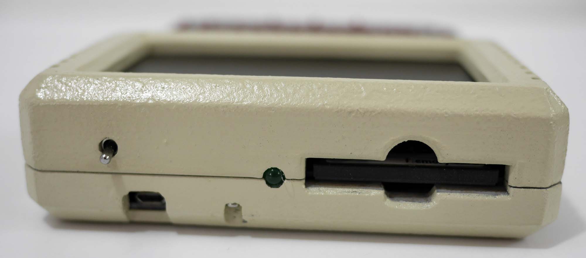
Top of unit contains power switch, micro USB charge port, disk activity LED and CompactFlash slot.
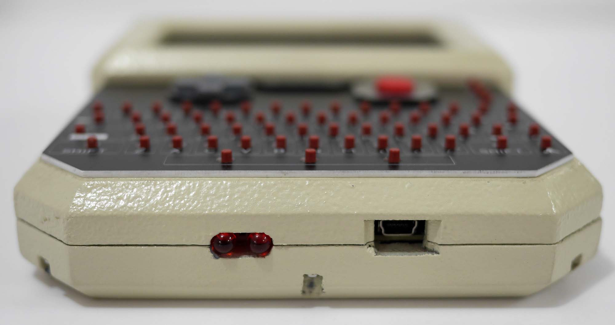
Bottom of unit contains Rx Tx indicator lights and the mini USB data transfer port. The Atari can actually handle speeds up to 57,600 baud, back in the day it was the slow disk drive limiting it to 19,200. (still faster than Commodore’s disk drive 🙂
Modern Atari-to-PC software can load a small bootloader in memory and then load the rest of your program at the higher rate of 57,000 baud.
Of course loading from the CompactFlash is much faster still as it’s a parallel 8 bit load not serial.
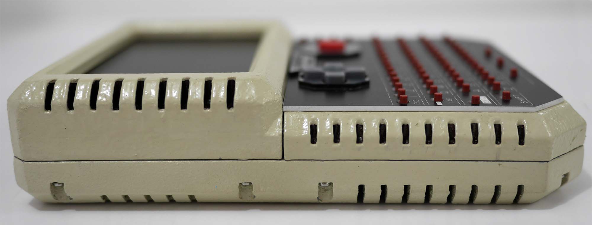
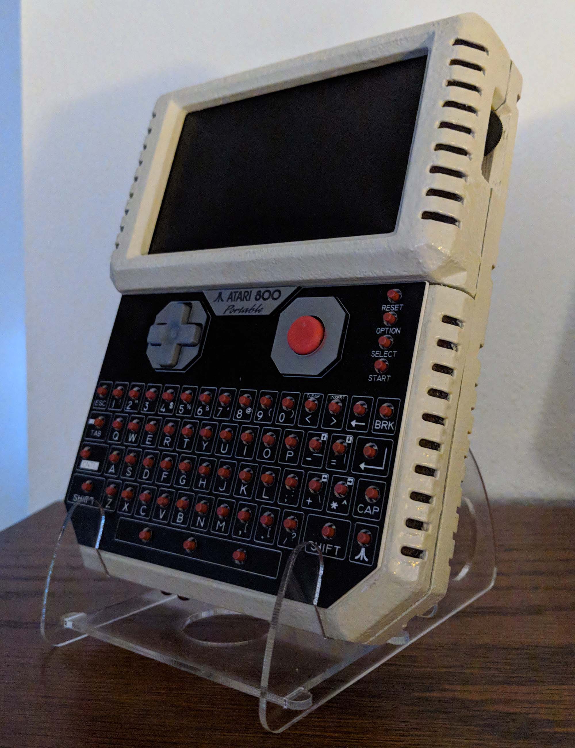
The joystick buttons are a little higher than they’d normally be but they needed to clear the keyboard. Also red wasn’t my first choice for tact switch color but what can you do?
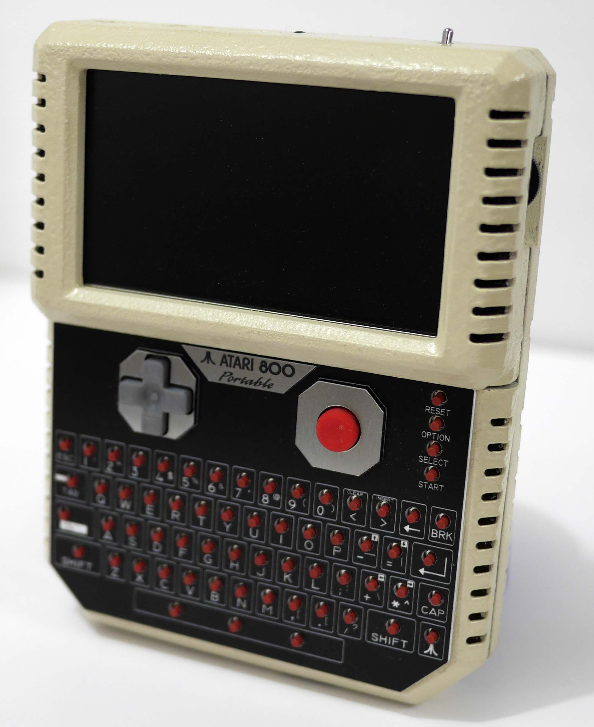
Only about half the air vents are real (mostly on the back). For the faux front ones Felix carefully painted black inside them to simulate the correct look. It looks a bit yellow in some of these photos but in real life it’s a very close match to the Atari 800XL.
The corresponding Ben Heck Show episodes: